- 您现在的位置:买卖IC网 > Sheet目录526 > SUD50N06-09L-E3 (Vishay Siliconix)MOSFET N-CH D-S 60V TO252
�� �
�
�SUD50N06-09L�
�Vishay� Siliconix�
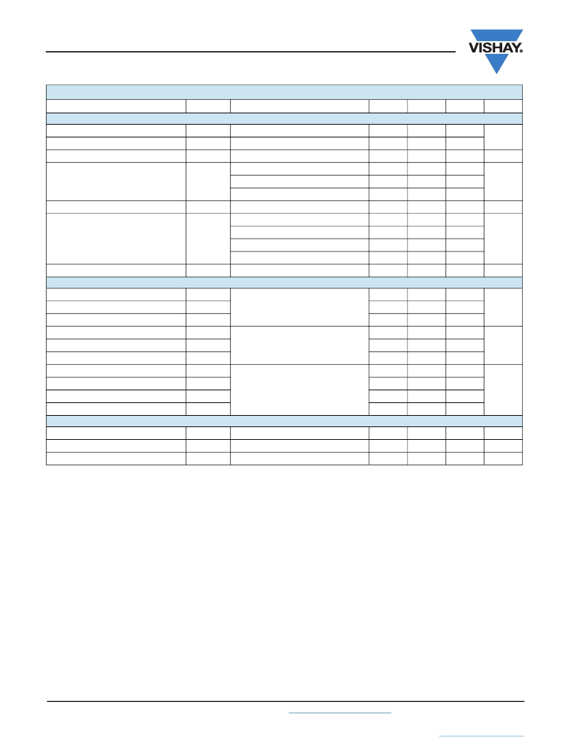
�SPECIFICATIONS� (T� J� =� 25� °C,� unless� otherwise� noted)�
�Parameter�
�Symbol�
�Test� Conditions�
�Min.�
�Typ.� a�
�Max.�
�Unit�
�Static�
�Drain-Source� Breakdown� Voltage�
�Gate� Threshold� Voltage�
�Gate-Body� Leakage�
�V� DS�
�V� GS(th)�
�I� GSS�
�V� GS� =� 0� V,� I� D� =� 250� μA�
�V� DS� =� V� GS� ,� I� D� =� 250� μA�
�V� DS� =� 0� V,� V� GS� =� ±� 20� V�
�60�
�1�
�2�
�3�
�±� 100�
�V�
�nA�
�V� DS� =� 60� V,� V� GS� =� 0� V�
�1�
�Zero� Gate� Voltage� Drain� Current�
�I� DSS�
�V� DS� =� 60� V,� V� GS� =� 0� V,� T� J� =� 125� °C�
�50�
�μA�
�V� DS� =� 60� V,� V� GS� =� 0� V,� T� J� =� 175� °C�
�250�
�On-State� Drain� Current� b�
�I� D(on)�
�V� DS� =� ?� 5� V,� V� GS� =� 10� V�
�V� GS� =� 10� V,� I� D� =� 20� A�
�50�
�0.0074�
�0.0093�
�A�
�Drain-Source� On-State� Resistance� b�
�R� DS(on)�
�V� GS� =� 10� V,� I� D� =� 20� A,� T� J� =� 125� °C�
�V� GS� =� 10� V,� I� D� =� 20� A,� T� J� =� 175� °C�
�0.0160�
�0.0200�
�?�
�V� GS� =� 4.5� V,� I� D� =� 15� A�
�0.0122�
�Forward� Transconductance�
�b�
�g� fs�
�V� DS� =� 15� V,� I� D� =� 20� A�
�60�
�S�
�Dynamic�
�Input� Capacitance�
�C� iss�
�2650�
�Output� Capacitance�
�Reverse� Transfer� Capacitance�
�Total� Gate� Charge� c�
�C� oss�
�C� rss�
�Q� g�
�V� GS� =� 0� V,� V� DS� =� 25� V,� f� =� 1� MHz�
�470�
�225�
�47�
�70�
�pF�
�Gate-Source�
�Charge� c�
�Q� gs�
�V� DS� =� 30� V,� V� GS� =� 10� V,� I� D� =� 50� A�
�10�
�nC�
�Gate-Drain� Charge� c�
�Q� gd�
�12�
�Turn-On� Delay� Time� c�
�t� d(on)�
�10�
�20�
�Rise� Time� c�
�Turn-Off� Delay� Time� c�
�Fall� Time� c�
�t� r�
�t� d(off)�
�t� f�
�V� DD� =� 30� V,� R� L� =� 0.6� ?�
�I� D� ?� 50� A,� V� GEN� =� 10� V,� R� g� =� 2.5� ?�
�15�
�35�
�20�
�25�
�50�
�30�
�ns�
�Source-Drain� Diode� Ratings� and� Characteristics� (T� C� =� 25� °C)�
�Pulsed� Current�
�I� SM�
�100�
�A�
�Diode� Forward� Voltage�
�Reverse� Recovery� Time�
�V� SD�
�t� rr�
�I� F� =� 20� A,� V� GS� =� 0� V�
�I� F� =� 20� A,� di/dt� =� 100� A/μs�
�1�
�45�
�1.5�
�100�
�V�
�ns�
�Notes:�
�a.� For� design� aid� only;� not� subject� to� production� testing.�
�b.� Pulse� test;� pulse� width� ?� 300� μs,� duty� cycle� ?� 2� %.�
�c.� Independent� of� operating� temperature.�
�Stresses� beyond� those� listed� under� “Absolute� Maximum� Ratings”� may� cause� permanent� damage� to� the� device.� These� are� stress� ratings� only,� and� functional� operation�
�of� the� device� at� these� or� any� other� conditions� beyond� those� indicated� in� the� operational� sections� of� the� specifications� is� not� implied.� Exposure� to� absolute� maximum�
�rating� conditions� for� extended� periods� may� affect� device� reliability.�
�Document� Number:� 72004�
�S13-0298-Rev.� F,� 11-Feb-13�
�For� technical� questions,� contact:� pmostechsupport@vishay.com�
�www.vishay.com�
�2�
�This� document� is� subject� to� change� without� notice.�
�THE� PRODUCTS� DESCRIBED� HEREIN� AND� THIS� DOCUMENT� ARE� SUBJECT� TO� SPECIFIC� DISCLAIMERS,� SET� FORTH� AT� www.vishay.com/doc?91000�
�发布紧急采购,3分钟左右您将得到回复。
相关PDF资料
SUD50N10-18P-GE3
MOSFET N-CH 100V DPAK
SUD50N10-34P-T4-E3
MOSFET N-CH D-S 100V TO252
SUD50NP04-77P-T4E3
MOSFET N/P-CH 40V TO252-4
SUD50P04-13L-E3
MOSFET P-CH D-S 40V TO252
SUD50P04-23-E3
MOSFET P-CH D-S 40V TO252
SUD50P04-40P-T4-E3
MOSFET P-CH D-S 40V TO252
SUD50P06-15L-T4-E3
MOSFET P-CH D-S 60V TO252
SUD50P08-26-E3
MOSFET P-CH D-S 80V TO252
相关代理商/技术参数
SUD50N06-09L-E3
制造商:Vishay Siliconix 功能描述:MOSFET
SUD50N06-12
制造商:Vishay Intertechnologies 功能描述:Trans MOSFET N-CH 60V 63A 3-Pin(2+Tab) DPAK
SUD50N06-12-E3
制造商:Vishay Intertechnologies 功能描述:Trans MOSFET N-CH 60V 63A 3-Pin(2+Tab) DPAK
SUD50N06-16
制造商:Vishay Intertechnologies 功能描述:Trans MOSFET N-CH 60V 50A 3-Pin(2+Tab) DPAK
SUD50N06-16-E3
制造商:Vishay Intertechnologies 功能描述:Trans MOSFET N-CH 60V 50A 3-Pin(2+Tab) DPAK
SUD50N06-36
制造商:VISHAY 制造商全称:Vishay Siliconix 功能描述:N-Channel 60-V (D-S), 150 °C MOSFET
SUD50N06-36-E3
制造商:Vishay Semiconductors 功能描述:
SUD50N06-36-T4-E3
功能描述:MOSFET 60V 12A 24W 36mohm @ 10V RoHS:否 制造商:STMicroelectronics 晶体管极性:N-Channel 汲极/源极击穿电压:650 V 闸/源击穿电压:25 V 漏极连续电流:130 A 电阻汲极/源极 RDS(导通):0.014 Ohms 配置:Single 最大工作温度: 安装风格:Through Hole 封装 / 箱体:Max247 封装:Tube